|
Derek Fountain : ZX Spectrum Expansion System Recreated
Programmer, Writer, Consultant, ZX Spectrum Peripheral Designer
|


|
|
|
|
|
|
|
|
|
|
|
|
|
|
|||

|
|||

|
|||

|
|||
In 1985 I used all my saved up money to buy a ZX Microdrive. I loved it. I was only kid in my school who could load a game in under 10 seconds. Ever since then the Microdrive has been, for me, the mass storage solution for the Spectrum. DivIDE is all fine and good, but it loses the Spectrum-ness of it all IMHO.
Sadly, the Microdrive tech is dying. We have a number of hardware-based Microdrive emulators, but they all emulate the tape drive itself and hence require an Interface One. The Interface One is becoming rare and expensive. Most people don't have one. The cartridges haven't stood the test of time, and they weren't hugely reliable to start with. There must be quite a few Spec-chums out there who've never loaded a game by typing "LOAD *" on a 48K's rubber keyboard. I find that sad. It's part of the ZX journey.
What the world needs, or at least what our little corner of the world needs, or at the very least what I want, is a device to plug into the back of a Spectrum which emulates an Interface One and Microdrive combination. Something that can load an MDR image (or 8) from SD card and present them such that "CAT 1", or "LOAD *" work as they should. Something that runs all the Microdrive compatible software from the 80s, that can load and save data as well as loading games. What I want, in short, is a properly emulated Microdrive expansion system backed by an SD card for storage of the MDR images.
So I made one. It looks like this:
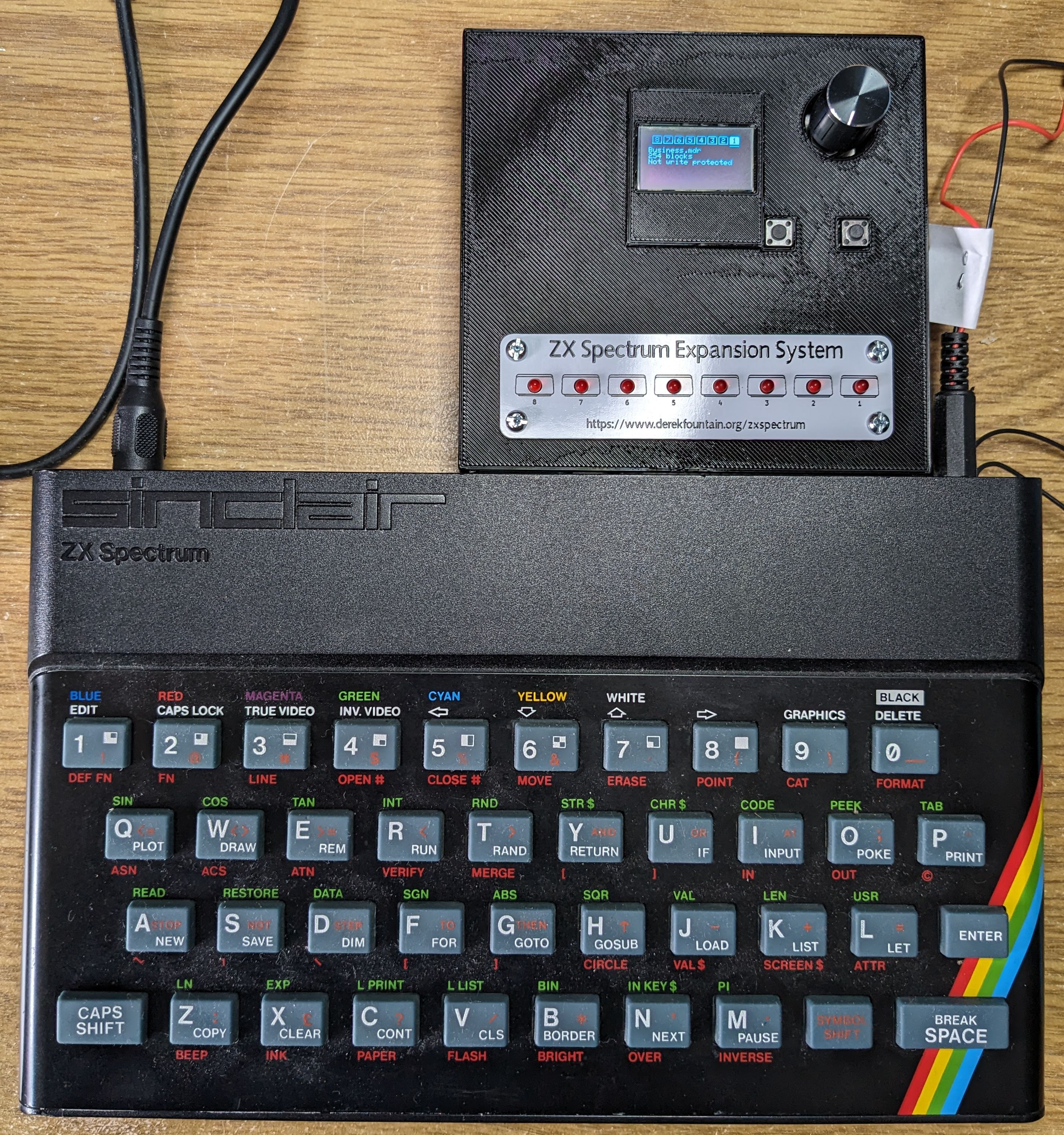
Here's a video demonstrating the device:
This is an open source and open hardware design project, licenced under GPL. The sources are on the Github page.
The rest of this article is a more technical look at the device, exploring the design and how it works.
The device is actually two boards, connected together with header pins and wrapped in a 3D printed case. The lower board carries most of the components.
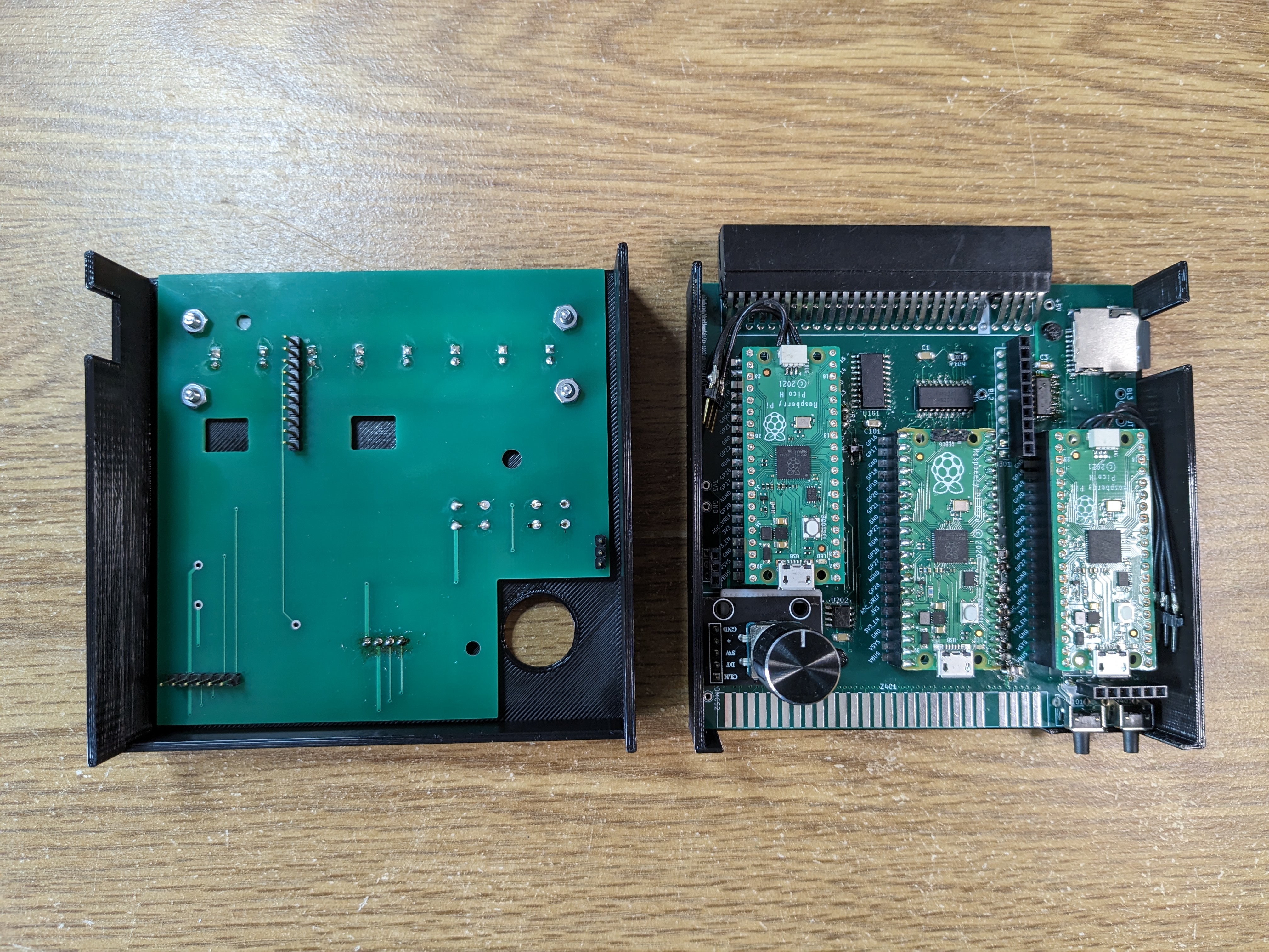
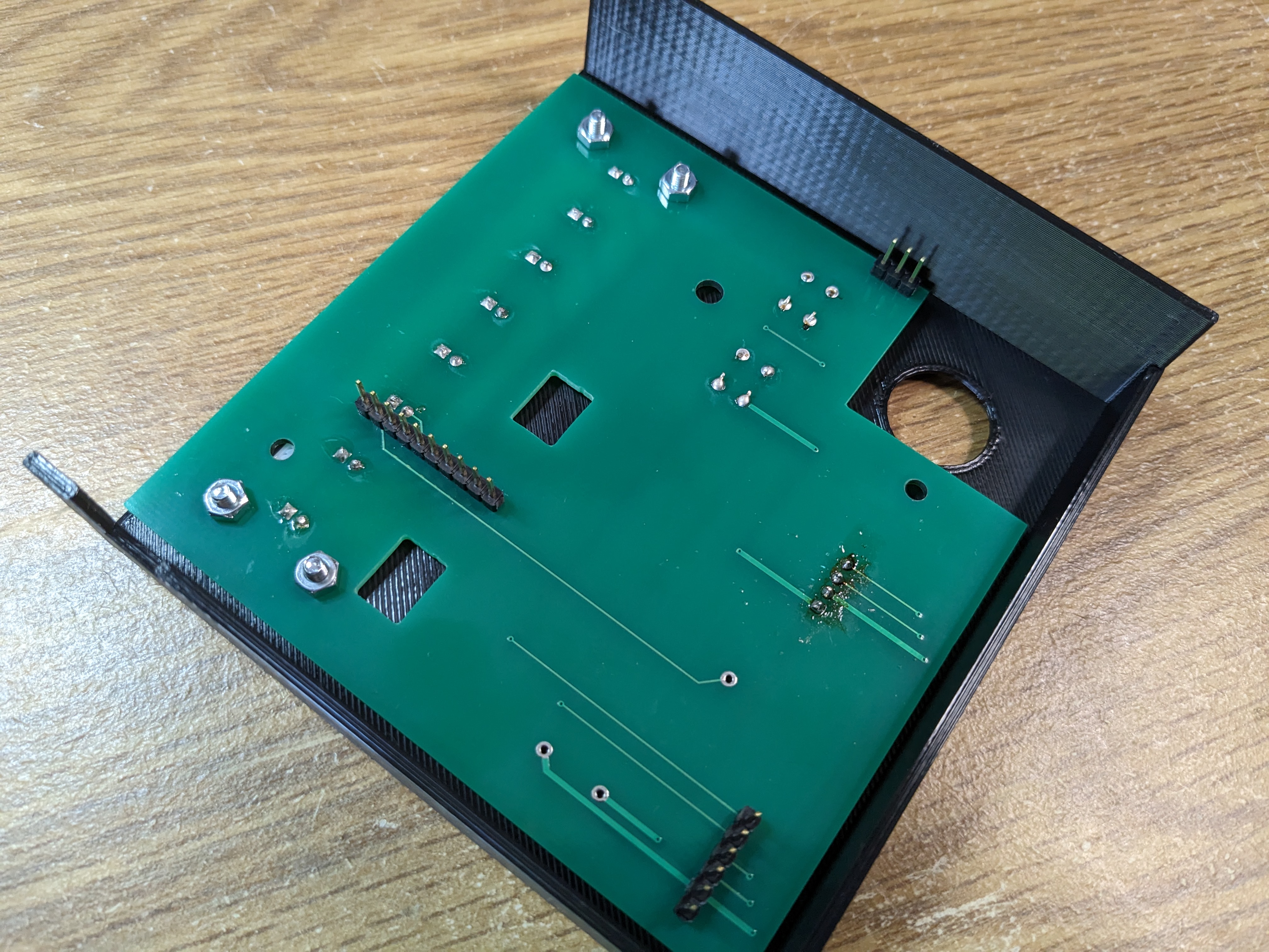
The top board has the OLED screen, two buttons ("action" and "cancel") and a row of red LEDs in the same style as that on the front of the original Microdrive. There's a faceplate with iconography to frame the LEDs. That's actually an aluminium PCB manufactured along with the other two by JLCPCB.
The lower board carries 3 Raspberry Pi Picos, and those are the devices which do all the work. The Picos are overkill, the RP2040 with a flash, a crystal and one or two other components all 3-times-over would do the job. The Pico has the advantage that it's very easy to physically work with.
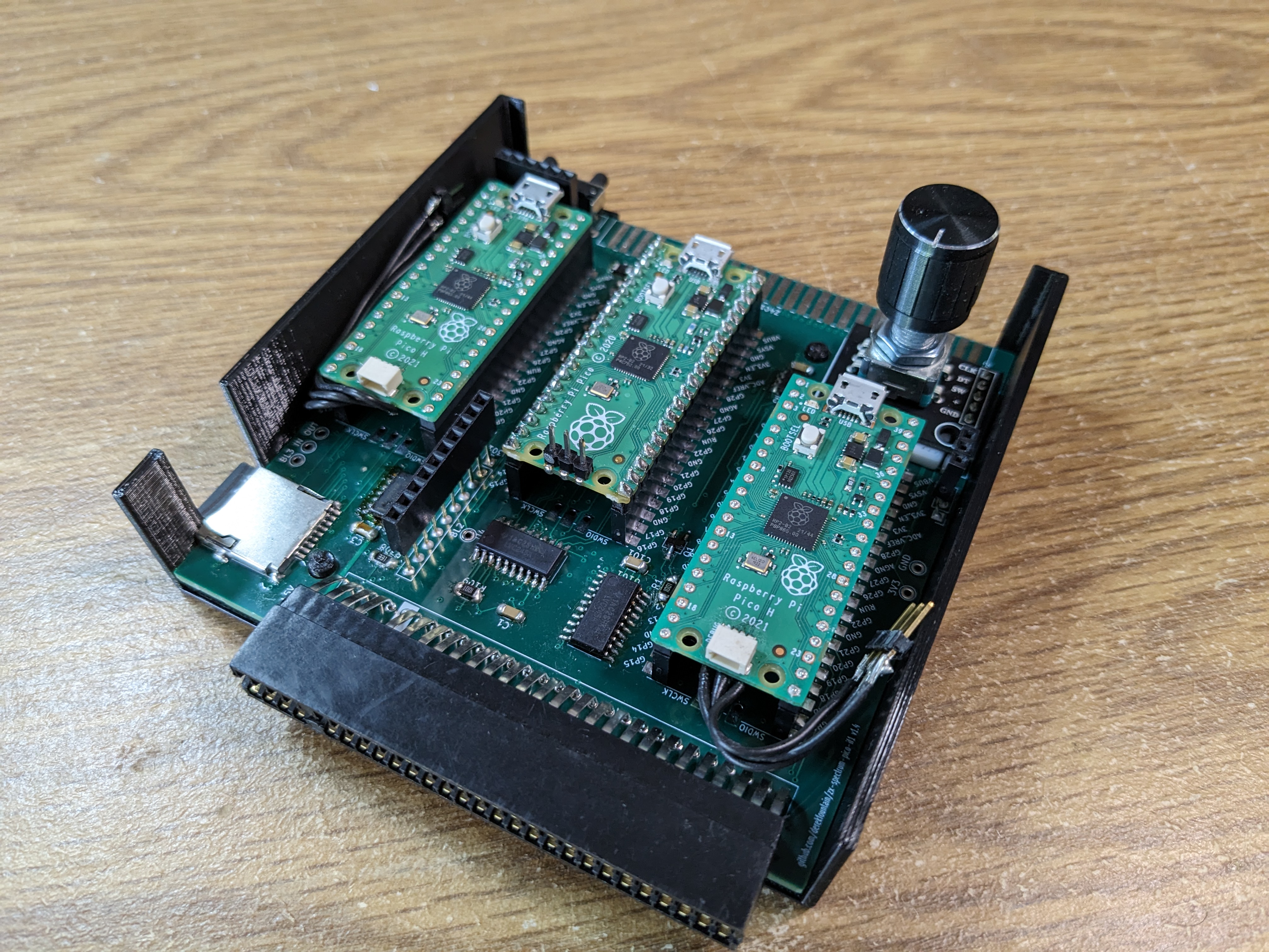
As well as the Picos, the lower board has the Spectrum connectors, the SD card reader, the rotary encoder and the reset buttons (one for the Z80 because it's useful, the other for all 3 Picos simultaneously in order to reset the whole device without disturbing the Z80).
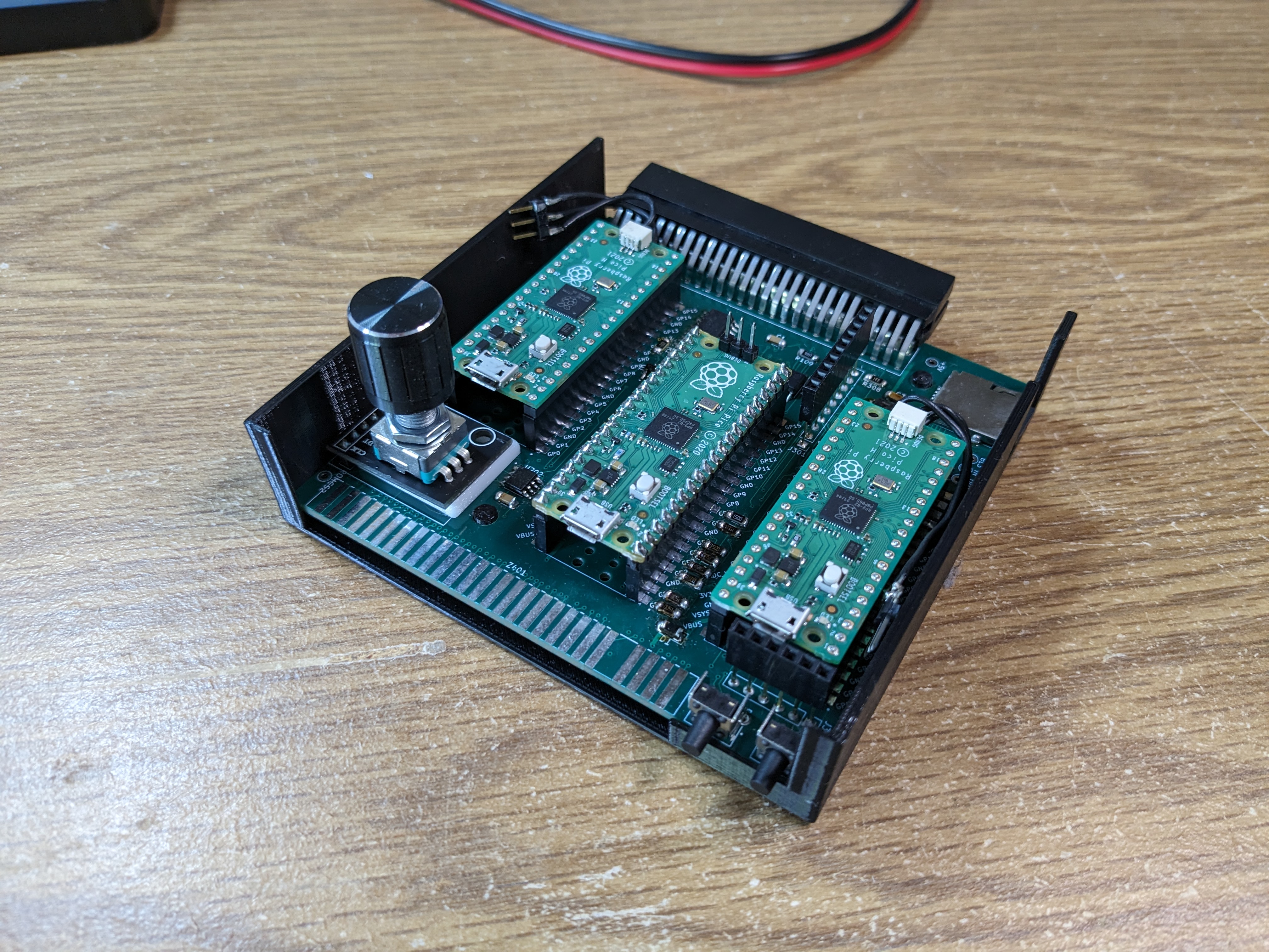
The Picos are each an embedded system in their own right. There is a bit of communication between them, which is detailed below.
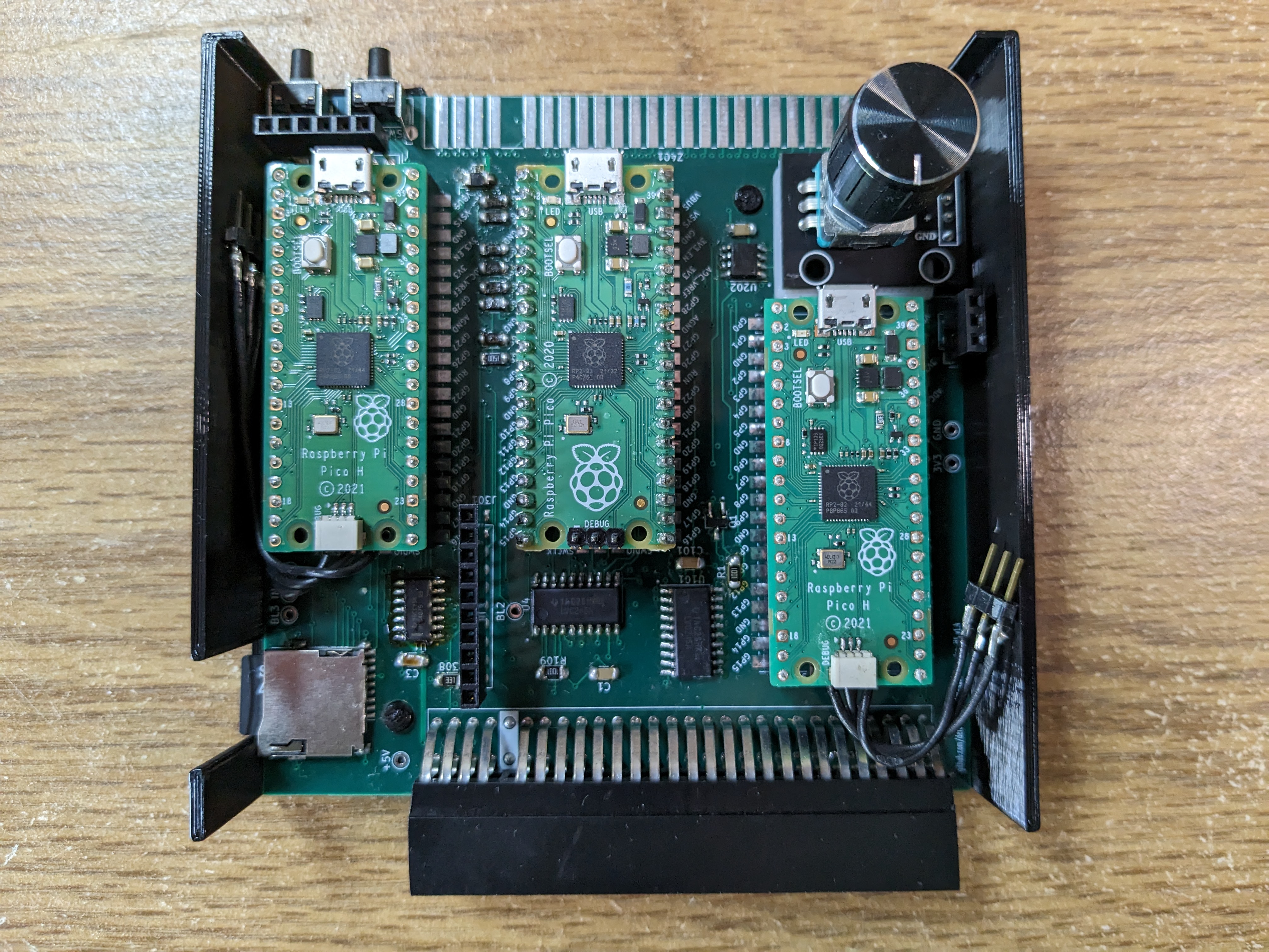
Pico 1 is mounted on the right side of the board as seen from the ZX Spectrum:
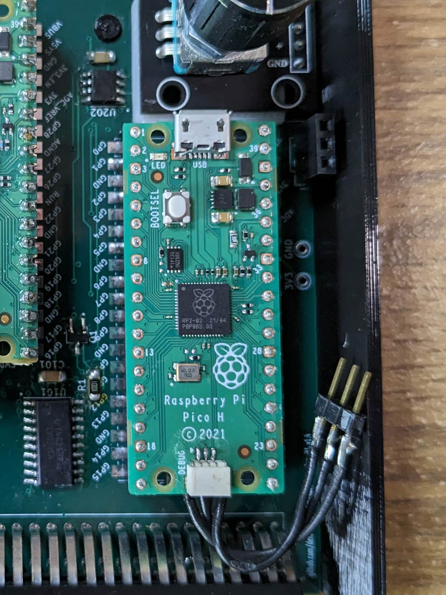
This Pico is the one which handles the Interface 1 ROM emulation. The Interface 1 has its own 8K ROM which contains the Z80 machine code to support the Microdrives and extended BASIC commands which control them. This Pico has a copy of this ROM, and ensures it is "paged in" when the normal Spectrum ROM hits its error handler routine. This design and code was originally implemented as part of my Pico ROM Interface project, so see there for more details.
Pico 1 uses its second core to play another important role. Pico 1 is the only one of the 3 Picos to have clear sight of the Z80's address bus. All the necessary address lines are connected to this Pico's GPIO pins. It turns out that Pico 2, which handles the IO and is described next, also needs some knowledge of the address lines so it can tell when the Z80 is doing IO to a relevant port. There aren't enough GPIOs free on Pico 2 for it to be able to see the address bus itself, so Pico 1 monitors the address lines and raises a single flag, in the form of a GPIO, which tells Pico 2 a relevant port is active on the address bus.
Pico 2 is mounted in the centre of the board:
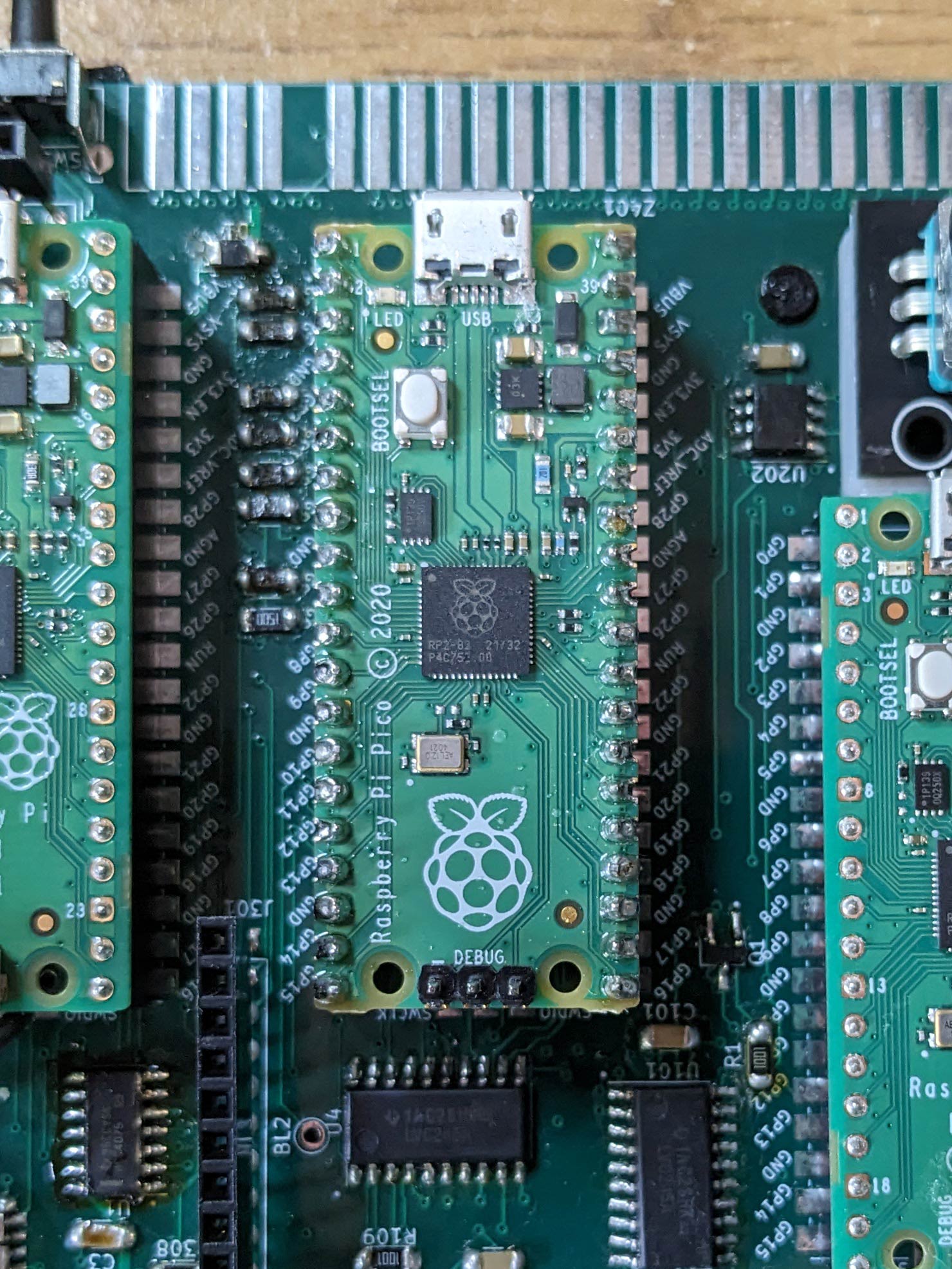
The second Pico, Pico 2, also known as the IO Pico, is the one which does the hard work. This Pico's primary role is to react to Z80 IO instructions - i.e. IN and OUT - when they are directed at IO ports which are relevant to the Interface 1. One of the RP2040 cores sits in a tight loop watching the data bus and /M1 lines which are connected to its GPIOs. When an IN or OUT instruction is on the data bus, and the address bus indicates the instruction is targeted at one of the Interface 1's IO ports (see discussion of that flag in the Pico 1 section above) the IO Pico asserts the Z80's /WAIT line, buying itself time to react to the Z80's instruction. An un-over-clocked RP2040 can't quite handle the instructions from the 3.5MHz Z80 quickly enough.
The Interface 1 uses just 4 IO ports:
- reading from port 0xEF sees the Interface 1 hardware return to the Z80 the status of the Microdrive;
- writing to port 0xEF allows the Z80 to control the Microdrive motors;
- reading from port 0xE7 sees the Interface 1 hardware return to the Z80 the data byte which is on the tape currently passing under the drive's read/write head;
- writing to port 0xE7 allows the Z80 to write a value onto the tape as it passes under the drive's read/write head.
That's the entire hardware interface to the 8 Microdrives. Everything else is done in software. That includes timings which control the data format on the tape, write protection, individual motor on or off signals, everything.
When I was planning the project, my first intention was to borrow one of the open source Microdrive emulation projects and add my own Interface 1 interface for it. I would, in essence, be reproducing the Interface 1 ULA, and I was bracing myself for some long nights staring at timing traces on the oscilloscope. Once I got started I had an epiphany. I didn't need to do that. I could go up a logical level and do all the data handling at the byte level from the MDR file. So for example, when the Z80 asks for the byte under the Microdrive's read/write head, I wouldn't try to work out what an emulated Microdrive was seeing, I could just go straight to the MDR file and read the byte from it as pointed to by a logical "head pointer", then increment the pointer ready for the next byte (simulating the tape moving on a bit). As it turns out, that's how the FUSE emulator does it, so I borrowed the code from that. The Microdrive simulation (it's not technically an emulation) in my IO Pico code started life as a a port of the Microdrive code from FUSE. Thanks guys!
In the top right of the image at the top of this section there's a small, 8 pin IC, U202. That is a serial memory chip, connected to the IO Pico over the SPI bus. The Pico has 264KB of RAM, but 8 Microdrive cartridges, at 135KB each, represents almost 1MB of storage online at any one time. I tried quite hard to find a way to hold this 1MB of data in the Pico's flash, switching the "active" cartridge image in and out of the Pico's RAM, but in the end gave up. Flash is just too slow, and since its writes work in 4KB chunks, it's very unwieldy. That serial RAM chip holds all 8 MDR images, and is fast enough to handle reads and writes directly within the Z80's instruction time (about 3.4 microseconds in the case of an IN).
The IC directly below the IO Pico in the above image is a level shifter. This converts data bus signals from the Spectrum's 5V to the Pico's 3.3V. A level shifter can only operate in one direction at a time, and this one is set such that data normally flows through it from the Spectrum towards the Pico. There are two instances, however, when the data needs to flow the other way. One is when the Z80 reads a byte from memory locations 0x0000 to 0x3FFF (i.e. it reads the ROM) and the other is when the Z80 reads one of the IO ports (i.e. it reads either Microdrive status, or the current Microdrive data byte). In these two instances the level shifter needs to be signalled to change direction. This is done by a small program running on one of the IO Pico's PIO processors. Inputs to this little program are from the ROM Pico, which indicates when it's handling a ROM read and needs the level shifter to allow data out. The other input is from the IO Pico itself when it wants to send a response to an IO port read back to the Spectrum. It's just a logical OR of the two signals, and I thought was going to have to add more logic circuitry to the board to support it. PIOs are wonderful things.
All of the above describes what the IO Pico is up to, but there's more. This Pico has another core and another PIO program running as well, but discussion of those will have to wait for the next section, the user interface Pico.
Pico 3, also known as the user interface, or UI Pico, is mounted on the left side of the board as seen from the ZX Spectrum:
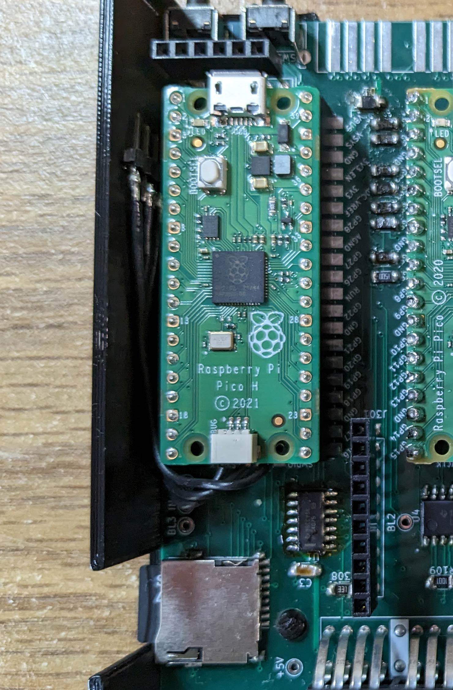
This Pico's first responsibility is to send and receive data to and from the IO Pico. The principal data package is the MDR file image, but there are other status and control packages which need to be sent back and forth as well. The first thing to discuss, then, is the communications link between the UI Pico and the IO Pico.
The first way I tried to do this was with SPI. I had an SPI bus free on the UI Pico, and one free on the IO Pico, and I already had everything configured because the serial RAM (discussed above) connected to the IO Pico is an SPI device. It should have been simple: set one end as master and the other as slave, and a 10mbps link appears. And, in fact, when I tried it, it did. But it didn't really work. SPI is frameless and driven by the master end. The slave could reply, but couldn't instigate messages. Even then I found messages were getting lost. I tried polling, I tried setting up interrupts, but each time I thought I'd got a working system I started seeing failures. Frustrating.
I gave up on SPI and switched to the more conventional approach of UARTs. These are much more reliable and designed for this sort of thing. The problem is they are a lot slower than SPI. The Pico hardware UARTs run at almost 1mbps, so a 135KB MDR image would transfer from Pico to Pico in about 1.5 seconds. I figured that was probably fast enough, but I couldn't get that to work reliably either. Bulk data went over just fine, but sending a 2 byte checksum would get lost. I could see those bytes on the wire on my oscilloscope (which does decoding) but the receiving Pico just didn't see them. Slowing the link down to 115,200bps worked fine with no changes to hardware or software. I didn't know what to make of it. More frustration,
Plan C was to use a Pico to Pico communications system developed by Andrew Menadue as part of his transputer emulation work. This uses a PIO at each end, and essentially bit bangs the bits of a byte on a single GPIO pin. Well, 2 GPIOs because I needed bidirectional communications. This approach works well. PIOs are very efficient and cost virtually nothing on the RP2040 core. They're fast too, my UI Pico and IO Pico converse at 10mbps so a 135KB MDR image transfers in about 650ms.
At the bottom of the image above is the SD card reader. The SD card carries the MDR files which would typically be saved onto it on a PC. The MDR file format is both open and well documented, so my expansion board retains compatibility with all Spectrum emulators which support MDR Microdrive files. The MDR file(s) selected by the user on the UI Pico are transferred across the PIO link to the IO Pico which puts them in the serial RAM it uses for Microdrive IO operations. When the IO Pico writes to the MDR image in the serial RAM it sends the image back to the UI Pico (discussed in a moment) which saves the MDR image back to the SD card.
(Some emulators, such as FUSE, have the user specifically saving modified MDR images back to disk, but I didn't like that idea. When a Spectrum writes data out to a Microdrive cartridge, the data goes straight onto the cartridge. I was aiming for a 100% replication of the original expansion system, so I always chose to emulate what the original device does as closely as possible.)
At the top of the image above there is a 6 pin header. That carries the signal to the OLED display which is an I2C device mounted on the top board. This header also carries the two push button signals, those switches also being mounted on the top board. The larger header to the bottom right carries the GPIO signals to the 8 LEDs.
The first core of the UI Pico runs the user interface. I'd never written a user interface before, so I had to make it up as I went along. I created a big state machine, so big in fact that I had to create a domain specific language to describe it, and tools to convert the DSL description of the user interface to 'C' code. Is that how people typically do these things? I've no idea, it's not normally my department. Anyway, one great big state machine with stimulus coming in from buttons and the rotary encoder and timers and other such places. But it works well.
The other core of this UI Pico manages a work queue. This work is based around a command pattern protocol which queues up tasks which need doing. Some are regular tasks, such as querying the IO Pico for status (which happens every 100ms). Others are more dynamic, such as sending an MDR image to the IO Pico telling it to "insert this cartridge" when the user selects an MDR file from the list. This point clears up the issue of what the second core on the IO Pico is doing: it's the receiving end of this command protocol, and is responsible for tasks such as receiving MDR images to insert, and telling the UI Pico that it's got written data which it needs to have saved back to the SD card.
This has been a reasonably high level view of how this device works. The definitive answers to all questions are, of course, in the source code. It is open source after all. Or you can just ask me. I'm happy to help anyone who's interested in the project.
Derek Fountain, July 2023
Site and content Copyright 2023 Derek Fountain - All Rights Reserved
